Lets talk about ECC and NAND flashes
Raw NAND flashes is not that common these days. At least not in those projects I have been working with for the last ~8 years. They seems to have been replaced by eMMC for many applications, but there are still some use cases where raw NAND flashes are prefered.
In this blog post, we will talk a little about Error Correcting Code (ECC) and NAND flashes as that is such a critical part of the NAND flash technology.
The goal is to show how to intepret the ECC positions in a datasheet and then translate it to a format that can be used in U-Boot and the Linux kernel.
Error Correction Codes
Error Correcting Code (ECC) is a method of detecting and correcting errors in data storage or transmission. All flash storages have a limited number of write cycles, and NAND flash is no exception. NAND flash is a type of non-volatile storage technology that does not require power to retain data. It is used in a variety of devices, including USB drives, memory cards, and solid-state drives (SSDs).
Common for all these types of devices is that they suffer from bit errors. These errors can be caused by a variety of factors, including electrical noise, temperature fluctuations, and wear and tear. To mitigate these errors, NAND flash devices use ECC to detect and correct errors in the data.
"That sounds complicated, lets stick to eMMC" you might say. But the truth is that an eMMC is "just" a managed NAND flash (so is also your USB drive, your SSD disk and ...) that do also suffer from these pecularities, but it is all hidden from the user. So instead of having control of how bad block management and ECC is handled, you simply have to trust the eMMC controller to do a good job.
Maybe it does, but maybe it doesn't. How do you know? You don't.
How does it work?
ECC is mathematical polynomial terms that are used to detect and correct errors in data. The ECC algorithm is used to generate a checksum for each block of data. The checksum is then stored in the flash memory along with the data. When the data is read back from the flash memory, the ECC algorithm is used to calculate a new checksum. If the new checksum does not match the stored checksum, an error has occurred, and the ECC algorithm is used to correct the error.
There are several different ECC algorithms that can be used with NAND flash, including Hamming code, Reed-Solomon code, and BCH code. The choice of ECC algorithm depends on the type of NAND flash and the level of error correction required. Usually you are forced to use a certain ECC algorithm (and layout) that the NAND flash controller supports, this to make the whole chain from ROM-bootloader up to the Linux kernel to use the same ECC algorithm. Otherwise you would not be able to, for example, to write the bootloader from Linux as it will generate a checksum that the ROM-bootloader will not be able to decode.
The strength of the ECC algorithm is measured in terms of the number of bits that can be corrected per block of data. For example, a 1-bit ECC algorithm can correct 1 bit of error per block, while a 2-bit ECC algorithm can correct 2 bits of error per block and so on. The stronger the ECC algorithm, the more bits of error it can correct, but it will introduce more overhead in terms of storage space.
What storage space by the way?
NAND flash layout
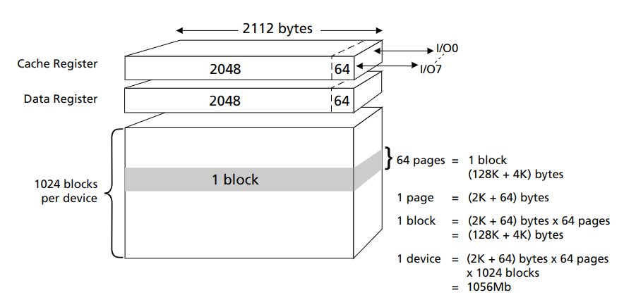
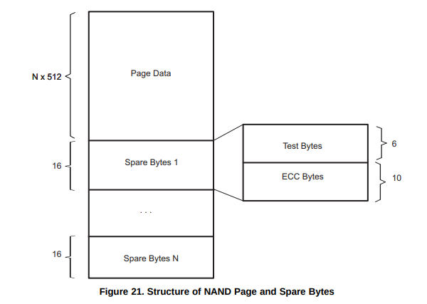
The NAND flash is organized in blocks and pages. All pages contains the actual data but also an Out Of Bound (OOB) area. The OOB area is used for storing metadata, such as ECC checksums, bad block markers, and other information. The size of the OOB area is typically 64 or 128 bytes per page, but it can vary depending on the NAND flash.
So when talking about that ECC occupy storage space, it is the OOB area that is referred to. The ECC checksums are stored in the OOB area, and the size of the ECC checksums depends on the ECC algorithm used.
You can read more about NAND flashes in a previous post [1].
Calculate ECC
The ECC can be calculated in hardware or software. In the case of hardware, it could be either the [2]:
- NAND flash controller in the SoC ("hw")
- NAND flash controller in the NAND flash ("on-die")
- Or an external ECC controller ("external")
that do the calculations.
In most cases, the OOB area will be used to store the ECC information. For example, the Micron MT29F1G08ABAFAWP flash chip has an (mandatory) 8-bit on-die ECC that stores the ECC information in the last 64 (of 128) bytes of the OOB area. Some NAND flashes with an on-die ECC could store the result in some secret place hidden from the user.
OOB layout
The OOB area is divided into several sections, including the ECC checksums, bad block markers, and other information. How the OOB area is divided depends on the NAND flash manufacturer and the ECC algorithm used. The expected layout is often hard-coded in the NAND flash controller, otherwise it would be hard for the ROM bootloader to use the NAND flash as a boot media as it would not know where to find nor decode the ECC checksums.
OOB-layout for the Davinci NAND-controller
The Davinci NAND controller is the nand controller that is used in both the Texas Instruments DA850 and KeyStone SoCs.
The ROM bootloader specifies the expected OOB layout in the datasheet for DA850 [3]:
And Keystone [4]:
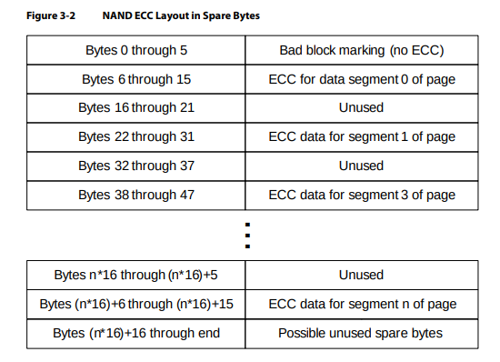
Which looks pretty much the same. This layout uses 10bit ECC per 512 chunk of data.
It is important to keep the same layout for all software that interract with the NAND flash. This usually includes the ROM bootloader, the Linux kernel and the U-Boot bootloader. If the layout is not the same, the ECC checksums will not be found nor decoded correctly, which results in read errors.
This is how the layout for this controller is represented in U-Boot [5]:
1#define CFG_SYS_NAND_ECCPOS		{				\
2				6, 7, 8, 9, 10, 11, 12, 13, 14, 15,	\
3				22, 23, 24, 25, 26, 27, 28, 29, 30, 31, \
4				38, 39, 40, 41, 42, 43, 44, 45, 46, 47, \
5				54, 55, 56, 57, 58, 59, 60, 61, 62, 63 }
6#define CFG_SYS_NAND_ECCSIZE		512
7#define CFG_SYS_NAND_ECCBYTES	10
And how it is represented in the Linux kernel:
 1static int hwecc4_ooblayout_large_free(struct mtd_info* mtd, int section,
 2                                      struct mtd_oob_region* oobregion)
 3{
 4       struct nand_device * nand = mtd_to_nanddev(mtd);
 5       unsigned int total_ecc_bytes = nand->ecc.ctx.total;
 6       int nregions = total_ecc_bytes / 10;
 7
 8       if (section >= nregions)
 9               return -ERANGE;
10
11       oobregion->offset = (section * 16) + 6;
12       oobregion->length = 10;
13
14       return 0;
15}
16
17static int hwecc4_ooblayout_large_free(struct mtd_info * mtd, int section,
18                                      struct mtd_oob_region * oobregion)
19{
20       struct nand_device * nand = mtd_to_nanddev(mtd);
21       unsigned int total_ecc_bytes = nand->ecc.ctx.total;
22       int nregions = total_ecc_bytes / 10;
23
24       if (section >= (nregions - 1))
25               return -ERANGE;
26
27       oobregion->offset = ((section + 1) * 16);
28       oobregion->length = 6;
29
30       return 0;
31}
32
33static const struct mtd_ooblayout_ops hwecc4_large_ooblayout_ops = {
34       .ecc = hwecc4_ooblayout_large_ecc,
35       .free = hwecc4_ooblayout_large_free,
36};
Surprisingly enough, this ECC layout was not supported in the Linux kernel but something I had to submit. It will be included in Linux 6.14 [6].
Summary
This is normally nothing you have to think of. Linux and many bootloaders already supports various NAND controllers and ECC-layouts so you only have to set which ECC mode you intend to use.
But sometimes that is not the case and you have to dig into the datasheet to figure out how the ECC is calculated and how it is stored in the NAND flash. Then it is better to know what you are looking for and how to intepret it.
References
| [1] | https://www.marcusfolkesson.se/blog/board-bring-up-part2/#nand-flash |
| [2] | https://git.kernel.org/pub/scm/linux/kernel/git/torvalds/linux.git/tree/Documentation/devicetree/bindings/mtd/raw-nand-chip.yaml?h=v6.13-rc7#n44 |
| [3] | https://www.ti.com/lit/an/sprab41f/sprab41f.pdf |
| [4] | https://www.ti.com/lit/ug/spruhj3/spruhj3.pdf |
| [5] | https://github.com/u-boot/u-boot/blob/master/include/configs/omapl138_lcdk.h#L115 |
| [6] | https://patchwork-proxy.ozlabs.org/project/linux-mtd/patch/20250109-davinci-nand-v2-1-06bc5a3d177a@gmail.com/ |