Board bring-up part 2: NAND flash
I'm currently working with a board bring up for a custom hardware based on a OMAPL138 from Texas Instruments. It is fun to work with "real" bring-ups. Most of my customers use System On Modules (SoM:s) these days. You get a lot for free with those modules but a lot of the fun is stripped away.
This post is not intended to be guide, it is more of a follow-me-through-my-work-post divided into three parts.
The first step is to get a bootloader to startup properly - which is also as far as I will take it in this series.
We are going to use U-boot [1] as bootloader for this project and I will use the TMDSLCDK138 [2] implementation as a reference during my bring-up, which is a evaluation kit for the OMAP-L138 CPU.
I will also be sharing lots of code snippets and it may not be obvious where they belong. In part4, I will summary all the changes I made.
About this part
Part 2 of this series will focus on the raw NAND flash which could be tricky to setup sometimes.
NAND flash
Lets talk about NAND flashes.
NAND flash memories is organized into blocks, pages and Out Of Bound (OOB) areas [3].
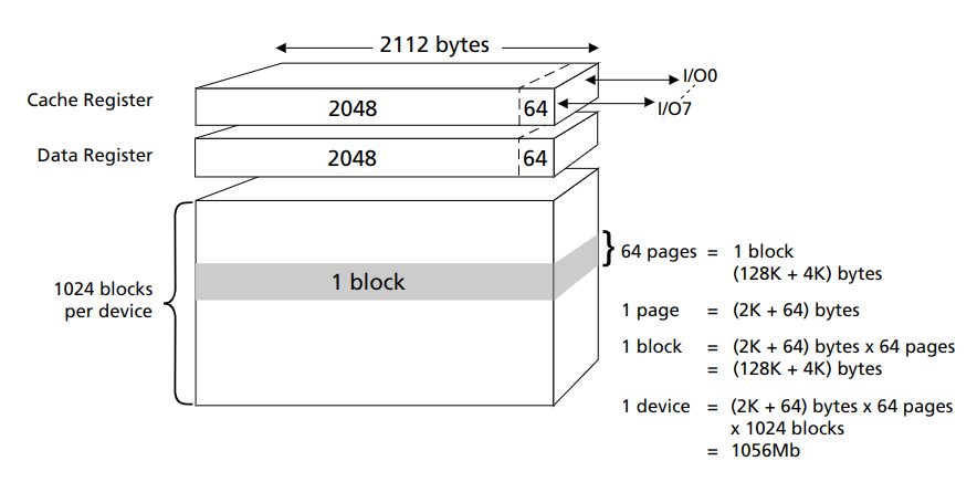
The smallest addressable unit in a NAND flash is a page, typically 2KB. Every page has a few extra spare bytes spare used to store metadata.
One block consists of 64 pages (2k page + 64 OOB) x 64 = 128k + 4k OOB in total.
MTD != Block devices
First, a MTD, Memory Technology Device, is not a block device.
They differ in many ways and needs to be threated differently from many aspects. Block devices has two main operations: read sector and write sector.
MTD devices on the other hand has three: read from eraseblock, write to eraseblock and erase eraseblock.
MTD devices (well, NAND devices) suffer from bad blocks, bit errors, wear leveling which block devices do not.
This affects which filesystems that are suitable for each type as the filesystem (or underlying layer, e.g. UBI) have to deal with this. Be aware of that many block devices, e.g. SSD, MMC, eMMC, USB drive flashes is usually (managed) NAND-flashes. The raw NAND is just hidden behind a (proprietary) Flash Translation Layer, FTL, that handles this for you.
You simply have to trust them to do it well.
OOB
OOB stands for out of band and is a spare area adjacent to the page The OOB area could be used by the filesystem, but the common usage of the area is to enable ECC (Error Correction Code) and bad block management.
ECC and bad blocks
As already mentioned, all NAND flashes have problem with data integrity, this problem is known as "bit errors".
The bit is stored as a voltage level in a cell, and many things can affect this voltage level. Charge leakage, read disturbance, cell-to-cell interference or cosmic radiation just mention a few. Bit errors will happened and the most efficient way to protect the data is by Error Correction Codes, ECCs.
There are many ECC algorithms out there, but the most commonly used is the Bose Chaudhuri Hocquenghem, BCH code. The ECC is usually, but not necessary, calculated in hardware. The hardware support could be in the CPU (as in this case) or in the NAND flash itself, so-called on-die. The number of bits in the ECC determines how many bitflips it could detect and correct.
OMAPL138 has hardware support for a 4bit ECC with an unknown algorithm - I cannot find anything about what algorithm they are using in the datasheet.
It is also important that all included components (bootloader, kernel) have the same idea about which ECC should be used and saved to which part of the OOB area. Otherwise, it is not possible to e.g. read data saved by U-boot in Linux.
Read out the OOB
So, with a basic understanding of how a NAND flash works, we can continue to dig into the problem; the data we read from the NAND flash is not correct.
When reading out a page from the NAND flash, the OOB area is validated to contain a block that is not bad. So lets add some tracers in the nand_is_bad_block() function. We print the whole OOB area.
 1static int nand_is_bad_block(int block)
 2{
 3	struct nand_chip *this = mtd_to_nand(mtd);
 4-	u_char bb_data[2];
 5+	u_char bb_data[64];
 6
 7	nand_command(block, 0, CONFIG_SYS_NAND_BAD_BLOCK_POS,
 8		NAND_CMD_READOOB);
 9
10	/*
11	 * Read one byte (or two if it's a 16 bit chip).
12	 */
13	if (this->options & NAND_BUSWIDTH_16) {
14		this->read_buf(mtd, bb_data, 2);
15		if (bb_data[0] != 0xff || bb_data[1] != 0xff)
16			return 1;
17	} else {
18		this->read_buf(mtd, bb_data, 64);
19+		printf("OOB\n\n");
20+		for (int i=0; i < 64; i++) {
21+			printf("%02x ", bb_data[i]);
22+			if (i % 8 == 0)
23+				printf ("\n");
24+		}
25
26		if (bb_data[0] != 0xff)
27			return 1;
28	}
29
30	return 0;
31}
The output I got was:
OOB:

 00 00 00 00 00 00 00 00
 00 00 00 00 00 00 00 00
 00 00 00 00 00 00 00 00
 00 00 00 00 00 00 00 00
 00 00 00 00 00 00 00 00
 00 00 00 00 00 00 00 00
 00 00 00 00 00 00 00 00
 00 00 00 00 00 00 00 00
Nope, that is not right.
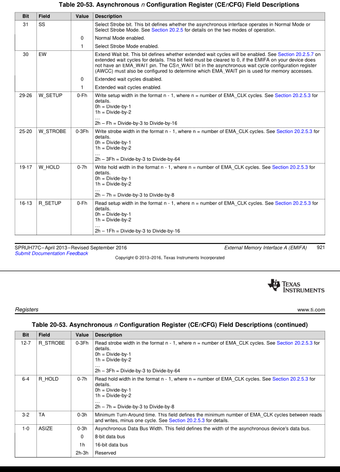
Change setup of the EMIFA controller
One thing that I found quite fast was that the configuration I used (based on the omapl138_lcdk board) does setup the EMIFA controller to work with 16 address bits for NAND flash, while my NAND flash only had 8 address bits.
So I changed the configuration accordingly:
 1#ifdef CONFIG_NAND_DAVINCI
 2       writel((DAVINCI_ABCR_WSETUP(15) |
 3               DAVINCI_ABCR_WSTROBE(63) |
 4               DAVINCI_ABCR_WHOLD(7) |
 5               DAVINCI_ABCR_RSETUP(15) |
 6               DAVINCI_ABCR_RSTROBE(63) |
 7               DAVINCI_ABCR_RHOLD(7) |
 8               DAVINCI_ABCR_TA(3) |
 9               DAVINCI_ABCR_ASIZE_8BIT),
10              &davinci_emif_regs->ab2cr);
11#endi
Still only reading out zeros:
OOB:

 00 00 00 00 00 00 00 00
 00 00 00 00 00 00 00 00
 00 00 00 00 00 00 00 00
 00 00 00 00 00 00 00 00
 00 00 00 00 00 00 00 00
 00 00 00 00 00 00 00 00
 00 00 00 00 00 00 00 00
 00 00 00 00 00 00 00 00
NAND Timing
Now we should setup a more proper timing to the NAND flash.
This is the required timing parameters @1V8:
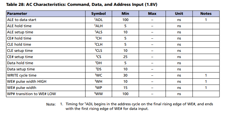
The PLL for the reference clock is 24MHz. SYSCLK3 is therefor 24/3 = 8MHz which is also what we use to clock the EMIFA module. One EMA_CLK cycle is therefor 125ns.
The register to set timing parameters for the EMIFA module is CE3CFG. Note that the values put into these registerns is a divider.
I ended up with this timing setup:
1    writel((DAVINCI_ABCR_WSETUP(2) |
2        DAVINCI_ABCR_WSTROBE(1) |
3        DAVINCI_ABCR_WHOLD(1) |
4        DAVINCI_ABCR_RSETUP(1) |
5        DAVINCI_ABCR_RSTROBE(3) |
6        DAVINCI_ABCR_RHOLD(2) |
7        DAVINCI_ABCR_TA(3) |
8        DAVINCI_ABCR_ASIZE_8BIT),
9           &davinci_emif_regs->ab2cr);
Now it looks better:
OOB:

 ff ff ff ff ff ff 89 fb
 01 77 59 ec b1 88 89 51
 ff ff ff ff ff ff 5a cf
 cd 4a 69 9d f4 c8 9f 62
 ff ff ff ff ff ff 88 e6
 38 b8 fa 08 35 0c 56 de
 ff ff ff ff ff ff 9e c3
 60 8d 7a 07 06 57 f2 358,
ECC
It is important to have the same ECC layout on both the kernel and bootloader side. This is the predefined layout when CONFIG_SYS_NAND_4BIT_HW_ECC_OOBFIRST=y in the configuration:
1#define CFG_SYS_NAND_ECCPOS		{				\
2				6, 7, 8, 9, 10, 11, 12, 13, 14, 15,	\
3				22, 23, 24, 25, 26, 27, 28, 29, 30, 31, \
4				38, 39, 40, 41, 42, 43, 44, 45, 46, 47, \
5				54, 55, 56, 57, 58, 59, 60, 61, 62, 63 }
6#define CFG_SYS_NAND_ECCSIZE		512
7#define CFG_SYS_NAND_ECCBYTES	10
Configuration
There are a few configurations related to NAND flash that I had to set:
- CONFIG_SYS_NAND_USE_FLASH_BBT=y: Use Bad Block Table stored in the OOB area.
- CONFIG_SYS_NAND_4BIT_HW_ECC_OOBFIRST=y: OOB/ECC layout
- CONFIG_SYS_NAND_PAGE_2K=y: Use 2k pages
- CONFIG_SYS_NAND_BLOCK_SIZE=0x20000: Block size is 128k
- CONFIG_SYS_NAND_PAGE_COUNT=0x40: 64 pages per block
- CONFIG_SYS_NAND_PAGE_SIZE=0x800: Each page is 2k
- CONFIG_SYS_NAND_OOBSIZE=0x40: OOB area for each page is 64 bytes
- CONFIG_SYS_NAND_BAD_BLOCK_POS=0: Bad block marker start at position 0
- CONFIG_SYS_NAND_U_BOOT_OFFS=0x100000: The U-Boot image should be read from address 0x100000
Read page data
The OOB data seems to be correct, but the board did still not boot U-boot.
I was just about to print the content of a page when I realized that the content is saved directly in the SDRAM which probably has the wrong timing setup... The OOB area is saved on the stack in the SRAM and thus works.
SDRAM Timing
Setup timing for the SDRAM is not an easy task. You need to know the calculated length of the trace paths to determine latencies and other effects.
Lucky for me, I managed to read out the SDRAM registers from another board. As the external RAM and board layout is the same, I could reuse them.
This is how I set up the DDR timing:
1#define CFG_SYS_DA850_DDR2_SDBCR2 0
2#define CFG_SYS_DA850_DDR2_SDTIMR (0x129129c8)
3#define CFG_SYS_DA850_DDR2_SDTIMR2 (0x380f7000)
4#define CFG_SYS_DA850_DDR2_SDRCR    0x0000040d
5#define CFG_SYS_DA850_DDR2_PBBPR    0x30
Another reboot
 1U-Boot SPL 2023.01-00822-g2051fcef92-dirty (Aug 19 2024 - 13:59:35 +0200)
 2Trying to boot from NAND
 3Loading U-Boot from 0x00100000 (size 0x00080000) to 0xc1080000
 4
 5
 6U-Boot 2023.01-00822-g2051fcef92-dirty (Aug 19 2024 - 13:59:35 +0200)
 7
 8Model: MFOC
 9DRAM:  128 MiB
10Core:  41 devices, 10 uclasses, devicetree: separate
11NAND:  128 MiB
12MMC:
13Loading Environment from NAND... OK
14In:    serial@10c000
15Out:   serial@10c000
16Err:   serial@10c000
17Net:   eth0: ethernet@220000
18Hit any key to stop autoboot:  0
It works. Nice.
Summary
NAND flashes could be tricky, but I've brought up so many board with different flash configurations in the past so it went very smoothly.
Continue to Part3 of this series.