Board bring-up part 1: Memory hassle
I'm currently working with a board bring up for a custom hardware based on a OMAPL138 from Texas Instruments. It is fun to work with "real" bring-ups. Most of my customers use System On Modules (SoM:s) these days. You get a lot for free with those modules but a lot of the fun is stripped away.
This post is not intended to be guide, it is more of a follow-me-through-my-work-post divided into three parts.
The first step is to get a bootloader to startup properly - which is also as far as I will take it in this series.
We are going to use U-boot [1] as bootloader for this project and I will use the TMDSLCDK138 [2] implementation as a reference during my bring-up, which is a evaluation kit for the OMAP-L138 CPU.
I will also be sharing lots of code snippets and it may not be obvious where they belong. In part4, I will summary all the changes I made.
About this part
This part will focus on the very first steps of the early bring-up. Basically from the start when I first got the hardware in my hands.
I leave out a lot of basic parts and focus more on what problems I encountered, my thoughts and how I solved them.
Most of this post is about an interresting problem I encountered and was debugging the wrong stuff for quite a long time. As always, the solution is obvious once you understand it and it's easy to stare blindly at the wrong direction. I think it is a funny problem to share.
The hardware
It is a new revision of a custom board that I should bring up. What you need to know for now is that it is equipped with:
- A new NAND flash (MT29F1G08ABADAWP) and
- A 1Gbit Mobile Low-Power DDR SDRAM (MT46H64M16LF).
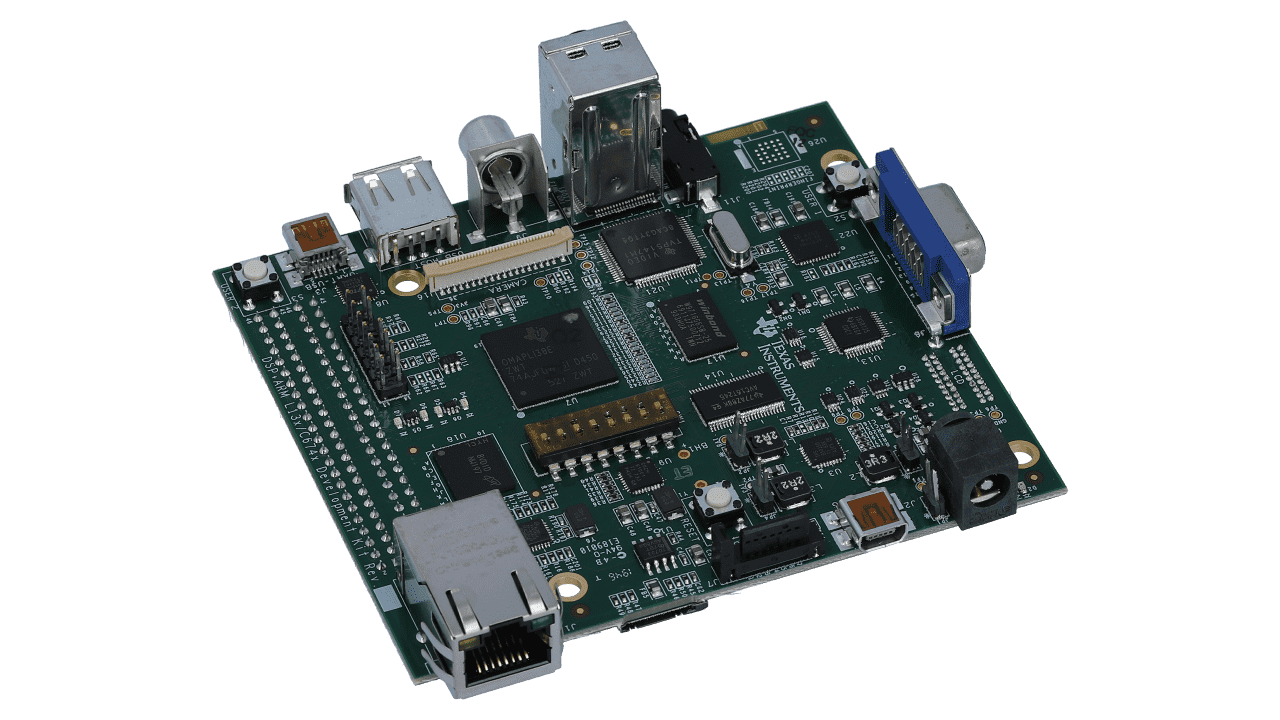
This is not the actual hardware I'm working with but the evaluation board (TMDSLCDK138) I'm using as a reference.
The boot process
To get a better understanding of the boot process, and the problem I encountered later on, I will describe the boot process for this particular CPU (applies for all SoCs in the DaVinci family).
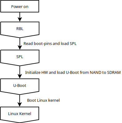
Stage 1: ROM Boot Loader
The initial bootloader which executes upon reset is the ROM Boot Loader (RBL) which is stored in the internal ROM.
The RBL is responsible to initialize the internal memory and then configure & initialize another controller (depending on pin configuration) to continue the boot process by loading the Secondary Program Loader (SPL).
In this case, the other controller is the EMIFA, External Memory Interface, to use with an external NAND flash.
Stage 2: Secondary Program Loader
The Secondary Program Loader (SPL) is responsible for initialize the system further. This include PLL configurations, the SDRAM controller, eventually a more fine grained initialization of the EMIFA controller and so on. The final goal is to load a full u-boot from a predefined location in a persistant storage (NAND flash in our case) to the SDRAM and then jump to the U-Boot entry point.
Stage 3: U-Boot
The final step in the boot process is U-boot itself. It is responsible to setup needed peripherals, load a kernel image to SDRAM and then continue from there.
Approach
I will start from the TMDSLCDK138 implementation, strip down what is not needed and adapt to my board. So I will basically build the omapl138-lcdk_defconfig configuration and see where it hits.
1$ make omapl138-lcdk_defconfig
2$ make CROSS_COMPILE=arm-linux-gnueabi- -j10
U-boot adds a generic AIS (Application Init Script) header to the SPL that is parsed by the RBL. You can read more about the AIS format in my previous post [5].
First attempt to boot
OMAPL-138 has different boot modes, one of those is the UART-mode where you use the UART to transfer the SPL to the internal SRAM and continue from there. This is the boot mode I will primary use during my development.
The first attempt to transfer the SPL to the SRAM ended up in... nothing.
No sign of life at all. Many questions were raised.
- Did the transfer suceed?
- Did the SPL execute at all?
- Does not the generic AIS header work on my board?
- Is it something with the toolchain?
I needed some way to verify that the SPL at least tried to execute.
I had limited resources in terms of debugging tools. I had no JTAG nor working serial port. At least a GPIO that I could toggle and measure on with the oscilloscope would have been helpful.
Work with GPIOs
There were no dedicated GPIOs that I could use for debugging, but I found a signal in the schematic which was also available in the design that I could use; GPIO 9 on Bank 5.
I consulted the datasheet to get the right addresses for the GPIO bank.
1#define GPIO_BANK4_REG_DIR_ADDR                (DAVINCI_GPIO_BASE + 0x60)
2#define GPIO_BANK4_REG_OPDATA_ADDR             (DAVINCI_GPIO_BASE + 0x64)
3#define GPIO_BANK4_REG_SET_ADDR                (DAVINCI_GPIO_BASE + 0x68)
4#define GPIO_BANK4_REG_CLR_ADDR                (DAVINCI_GPIO_BASE + 0x6c)
And how to MUX the pin:
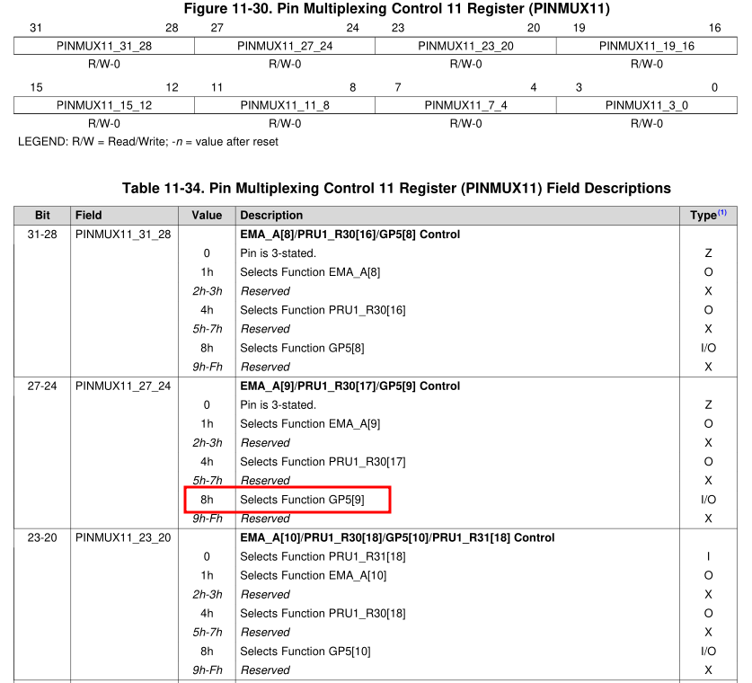
So I ended up with this code snippet in spl_board_init(void).
 1const struct pinmux_config gpio_pins[] = {
 2    { pinmux(11), 8, 6 }
 3};
 4
 5davinci_configure_pin_mux_items(pinmuxes, ARRAY_SIZE(gpio pins));
 6
 7   /* Set the GPIO direction as output */
 8clrbits_le32((u32 *)GPIO_BANK4_REG_DIR_ADDR, (0x01 << 25));
 9
10/* Set the output as low */
11writel(0x01 << 25, GPIO_BANK4_REG_CLR_ADDR);
12__udelay(10);
13/* Set the output as high */
14writel(0x01 << 25, GPIO_BANK4_REG_SET_ADDR);
15__udelay(10);
16/* Set the output as low */
17writel(0x01 << 25, GPIO_BANK4_REG_CLR_ADDR);
18__udelay(10);
19/* Set the output as high */
20writel(0x01 << 25, GPIO_BANK4_REG_SET_ADDR);
21__udelay(10);
22/* Set the output as low */
23writel(0x01 << 25, GPIO_BANK4_REG_CLR_ADDR);
It worked! The SPL does actually execute!
Stuck at reading from NAND flash
The Secondary Program Loader (SPL) starts, but once it should load the full u-boot from NAND flash it got stuck. The only debugging tools I had was a GPIO. I came quite long with this only GPIO though. Long enough to determine that:
- The SPL was successfully loaded by the RBL from NAND flash and was actually executing (which is a huge success).
- I could follow the code path with a lot of creative toggle patterns down to the code part that actually reads from the NAND flash where it got stuck.
Now I need better tools to debug this, so I started to work on getting an early UART to work.
Talk to me, please
The registers to setup for the UART module in the OMAPL138 is compatible with NS16550 [3], which is a semi-standard for UART implementations. This makes it quite straigt forward to get the UART up and running.
What I basically had to do was setup proper pinmux for the UART1:
 1static const struct pinmux_config uart_pins[] = {
 2	{ pinmux(4), 2, 4 },
 3	{ pinmux(4), 2, 5 }
 4};
 5
 6const struct pinmux_resource pinmuxes[] = {
 7	PINMUX_ITEM(uart_pins),
 8};
 9
10int board_early_init_f(void)
11{
12    davinci_configure_pin_mux_items(pinmuxes, ARRAY_SIZE(pinmuxes));
13    return 0;
14}
Enable the power domain:
1lpsc_on(DAVINCI_LPSC_UART1);Register a ns16550 device to be used by SPL:
 1static const struct ns16550_plat serial_pdata = {
 2	.base = DAVINCI_UART1_BASE,
 3	.reg_shift = 2,
 4	.clock = 228000000,
 5	.fcr = UART_FCR_DEFVAL,
 6};
 7
 8U_BOOT_DRVINFO(omapl138_uart) = {
 9	.name = "ns16550_serial",
10	.plat = &serial_pdata,
11};
And make sure that I had enabled the relevant configurations:
1$ grep SPL_.*SERIAL .config
2CONFIG_SPL_SERIAL=y
3CONFIG_SPL_SERIAL_PRESENT=y
4CONFIG_SPL_DM_SERIAL=y
I was so happy when I finally got this to my terminal:
1U-Boot SPL 2023.01-00827-gc342c012a7 (Aug 14 2024 - 13:28:38 +0200)
2Trying to boot from NAND
3Loading U-Boot from 0x00100000 (size 0x00080000) to 0xc1080000
The MTD/NAND flash implementation
I use the simple implementation for the NAND flash (CONFIG_SPL_NAND_SIMPLE=y).
The driver, drivers/mtd/nand/raw/nand_spl_simple.c, declares two structures used for all interactions with the NAND flash:
1static struct mtd_info *mtd;
2static struct nand_chip nand_chip;
The structures are similiar to those you find in the Linux kernel. The struct nand_chip contains a bunch of callback functions:
 1struct nand_chip {
 2	struct mtd_info mtd;
 3	struct nand_id id;
 4
 5	void __iomem *IO_ADDR_R;
 6	void __iomem *IO_ADDR_W;
 7
 8	ofnode flash_node;
 9
10	uint8_t (*read_byte)(struct mtd_info *mtd);
11	u16 (*read_word)(struct mtd_info *mtd);
12	void (*write_byte)(struct mtd_info *mtd, uint8_t byte);
13	void (*write_buf)(struct mtd_info *mtd, const uint8_t *buf, int len);
14	void (*read_buf)(struct mtd_info *mtd, uint8_t *buf, int len);
15	void (*select_chip)(struct mtd_info *mtd, int chip);
16	int (*block_bad)(struct mtd_info *mtd, loff_t ofs);
17	int (*block_markbad)(struct mtd_info *mtd, loff_t ofs);
18	void (*cmd_ctrl)(struct mtd_info *mtd, int dat, unsigned int ctrl);
19	int (*dev_ready)(struct mtd_info *mtd);
20	void (*cmdfunc)(struct mtd_info *mtd, unsigned command, int column,
21			int page_addr);
22	int(*waitfunc)(struct mtd_info *mtd, struct nand_chip *this);
23	int (*erase)(struct mtd_info *mtd, int page);
24	int (*scan_bbt)(struct mtd_info *mtd);
25	int (*write_page)(struct mtd_info *mtd, struct nand_chip *chip,
26			uint32_t offset, int data_len, const uint8_t *buf,
27			int oob_required, int page, int raw);
28	int (*onfi_set_features)(struct mtd_info *mtd, struct nand_chip *chip,
29			int feature_addr, uint8_t *subfeature_para);
30	int (*onfi_get_features)(struct mtd_info *mtd, struct nand_chip *chip,
31			int feature_addr, uint8_t *subfeature_para);
32	int (*setup_read_retry)(struct mtd_info *mtd, int retry_mode);
33	int (*setup_data_interface)(struct mtd_info *mtd, int chipnr,
34				    const struct nand_data_interface *conf);
35
36	[...]
37
38};
Defined by davinci_nand_init() in the generic board_nand_init() function that you find in drivers/mtd/nand/raw/davinci_nand.c:
1int board_nand_init(struct nand_chip *chip)
2{
3	davinci_nand_init(chip);
4	return 0;
5}
Wierd things is going on...
As soon as any of these callback functions were used, things starts getting really wierd. Sometimes it works, sometimes it not.
I printed and compared the addresses of the callback function with the addresses of the actual functions. It looked good. So what is going on?
I observed one strange thing though; as soon as I pass the mtd or nand_chip structure by pointer to a function (e.g. board_nand_init()), that changes internal values of the struct, it does not always come back changed.
A simplified example would be:
 1void foo(struct nand_chip *chip)
 2{
 3	chip->foobar = 35;
 4}
 5
 6void bar()
 7{
 8	nand_chip->foobar = 20;
 9	foo(nand_chip);
10
11	/* nand_chip->foobar is still 20.. SOMETIMES? */
12}
I did so many tests and even began to doubt my pointer-fu.
What concerned me was that I got quite far in the boot process, so many things worked just fine... but not these two structures.
So I started to look into the map file to see where these structures are located in the ELF file.
1$ grep nand_chip -A 5  spl/u-boot-spl.map
2 .bss.nand_chip
3                0x00000018      0x558 drivers/mtd/nand/raw/nand_spl_simple.o
4 .bss.mtd       0x00000570        0x4 drivers/mtd/nand/raw/nand_spl_simple.o
5                0x00000574                        . = ALIGN (0x4)
6                0x00000574                        __bss_end = .
The structures sits in the BSS segment, that is expected as they are a static unitialized structures, but the address caught my eye.
The .bss.nand_chip structure is located at address 0x00000018. Lets talk about the memory layout for the OMAPL138.
Memory layout of OMAPL138
The RBL loads the SPL to the internal RAM, which is the Shared RAM starting at 0x80000000 in the memory layout.
The DDR2/mDDR memory area on the other hand, starts at 0xC0000000 as you can read in the datasheet [4]:
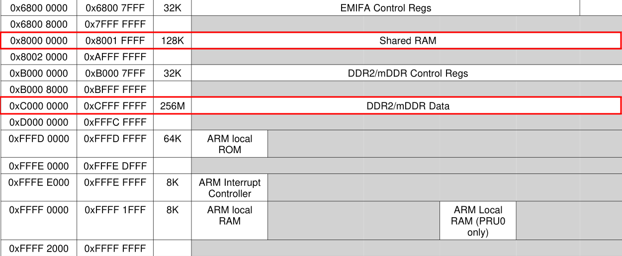
Usually, resources located in the external RAM is addressed from 0x00000000.
Lets have a look at the nand functions used as callbacks. Those should be located in the .TEXT segment which sits in the SRAM for sure:
 1$ grep -A2 nand_davinci spl/u-boot-spl.map
 2 .text.nand_davinci_read_buf
 3                0x80002888       0x4c drivers/mtd/nand/raw/davinci_nand.o
 4 .text.nand_davinci_write_buf
 5                0x800028d4       0x4c drivers/mtd/nand/raw/davinci_nand.o
 6 .text.nand_davinci_hwcontrol
 7                0x80002920       0x2c drivers/mtd/nand/raw/davinci_nand.o
 8 .text.nand_davinci_dev_ready
 9                0x8000294c       0x10 drivers/mtd/nand/raw/davinci_nand.o
10 .text.nand_davinci_4bit_enable_hwecc
11                0x8000295c       0x30 drivers/mtd/nand/raw/davinci_nand.o
12 .text.nand_davinci_4bit_correct_data
13                0x8000298c      0x184 drivers/mtd/nand/raw/davinci_nand.o
14 .text.nand_davinci_4bit_calculate_ecc
15                0x80002b10       0x88 drivers/mtd/nand/raw/davinci_nand.o
16 .text.board_nand_init
17--
18 .data.nand_davinci_4bit_layout_oobfirst
19                0x800037b0      0xba8 drivers/mtd/nand/raw/davinci_nand.o
Those addresses starts with 0x8000xxxx as expected.
So the .BSS segment sits in the external SDRAM then. That is a clue!
You could have figured that out on your own. There is no need to take up space in the internal RAM for the BSS segment. Especially not when one of the tasks of the SPL is to configure the external memory so that it is available.
Linker script
Lets look into the linker script (board/davinci/da8xxevm/u-boot-spl-da850evm.lds, set by CONFIG_SPL_LDSCRIPT) used by the SPL:
 1MEMORY { .sram : ORIGIN = IMAGE_TEXT_BASE,\
 2		LENGTH = CONFIG_SPL_MAX_FOOTPRINT }
 3
 4MEMORY { .sdram : ORIGIN = CONFIG_SPL_BSS_START_ADDR, \
 5                LENGTH = 0x1080000 }
 6
 7OUTPUT_FORMAT("elf32-littlearm", "elf32-littlearm", "elf32-littlearm")
 8OUTPUT_ARCH(arm)
 9ENTRY(_start)
10SECTIONS
11{
12	. = 0x00000000;
13
14	. = ALIGN(4);
15	.text      :
16	{
17	__start = .;
18	  *(.vectors)
19	  arch/arm/cpu/arm926ejs/start.o	(.text*)
20	  *(.text*)
21	} >.sram
22
23	. = ALIGN(4);
24	.rodata : { *(SORT_BY_ALIGNMENT(.rodata*)) } >.sram
25
26	. = ALIGN(4);
27	.data : { *(SORT_BY_ALIGNMENT(.data*)) } >.sram
28
29	. = ALIGN(4);
30	__u_boot_list : { KEEP(*(SORT(__u_boot_list*))); } >.sram
31
32	. = ALIGN(4);
33	.rel.dyn : {
34		__rel_dyn_start = .;
35		*(.rel*)
36		__rel_dyn_end = .;
37	} >.sram
38
39	__image_copy_end = .;
40
41	.end :
42	{
43		*(.__end)
44	}
45
46	_image_binary_end = .;
47
48	.bss :
49	{
50		. = ALIGN(4);
51		__bss_start = .;
52		*(.bss*)
53		. = ALIGN(4);
54		__bss_end = .;
55	} >.sdram
56}
IMAGE_TEXT_BASE=0x80000000 and CONFIG_SPL_BSS_START_ADDR=0xC0000000
As we can see, we reserve a a bit of the external RAM for the SPL:
1MEMORY { .sdram : ORIGIN = CONFIG_SPL_BSS_START_ADDR, \
2                LENGTH = 0x1080000 }
To be used for the BSS segment:
1	.bss :
2	{
3		. = ALIGN(4);
4		__bss_start = .;
5		*(.bss*)
6		. = ALIGN(4);
7		__bss_end = .;
8	} >.sdram
Just test to put the BSS segment into the SRAM instead:
1	.bss :
2	{
3		. = ALIGN(4);
4		__bss_start = .;
5		*(.bss*)
6		. = ALIGN(4);
7		__bss_end = .;
8-	} >.sdram
9+	} >.sram
Rebuild U-Boot and verify with the map file:
1$ grep nand_chip -A 5  spl/u-boot-spl.map
2 .bss.nand_chip
3                0x800045e8      0x558 drivers/mtd/nand/raw/nand_spl_simple.o
4 .bss.mtd       0x80004b40        0x4 drivers/mtd/nand/raw/nand_spl_simple.o
5                0x80004b44                        . = ALIGN (0x4)
6                0x80004b44                        __bss_end = .
Great!
Another try to load the image
The part of the code that loads the U-Boot image, nand_spl_load_image(), from the NAND flash did finally return! It did not hang in the middle of somewhere!
 1static int spl_nand_load_image(struct spl_image_info *spl_image,
 2			struct spl_boot_device *bootdev)
 3{
 4	nand_init();
 5
 6	printf("Loading U-Boot from 0x%08x (size 0x%08x) to 0x%08x\n",
 7	       CONFIG_SYS_NAND_U_BOOT_OFFS, CFG_SYS_NAND_U_BOOT_SIZE,
 8	       CFG_SYS_NAND_U_BOOT_DST);
 9
10	nand_spl_load_image(spl_nand_get_uboot_raw_page(),
11			    CFG_SYS_NAND_U_BOOT_SIZE,
12			    (void *)CFG_SYS_NAND_U_BOOT_DST);
13	spl_set_header_raw_uboot(spl_image);
14	nand_deselect();
15
16	/* WE GOT HERE! */
17
18	return 0;
19}
Summary
The configuration of the mDDR2 memory was the culprit all along.
I probably would have discovered it earlier if I didn't know that the same mDDR memory is used in the previous revision of the board, while the NAND flash is completely new in this design.
That made me turn all my attention to the NAND flash. As if by chance, it was precisely those structures that gave me trouble.
Continue to Part2 of this series.